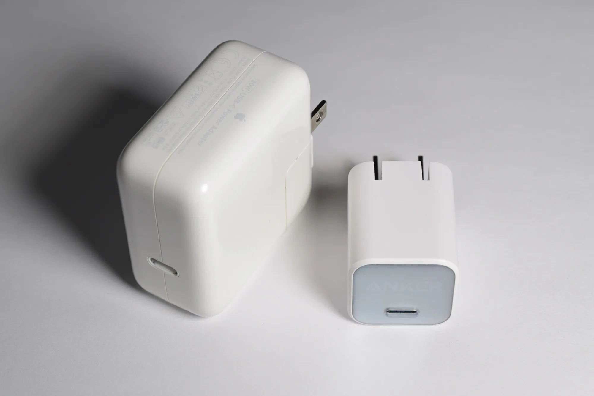
Size comparison of Si vs GaN USB-C chargers at the same wattage. Photo: 4300streetcar, 2025-12-25. License via Wikimedia Commons.
30-second overview: In the fourth quarter of 2025, TSMC began 2-nanometer mass production at Kaohsiung Fab 22, leading the world by two to three generations1. But the story is not only about transistors getting smaller: the fast charger in your bag contains gallium nitride (GaN), GlobalWafers is making 8-inch silicon carbide (SiC) wafers in Zhongli, and NVIDIA's Blackwell GPUs all depend on TSMC's CoWoS packaging to enter data centers. From ITRI spending US$4.5 million in 1973 to buy technology from RCA2, to Academia Sinica connecting a 20-qubit superconducting quantum chip to the internet in 20263, Taiwan has traveled a long river of materials science, from bandgap physics to atomic layer deposition to topological qubits. The sacred mountain protecting the nation rests on fifty years of foundry experience, but Taiwan has not yet secured its foundry position for the quantum era.
One afternoon in 1985, Minister without Portfolio K.T. Li met Morris Chang at the Executive Yuan. Chang had just returned to Taiwan to take over as president of ITRI. Li came straight to the point: "We want to build a very large-scale integrated circuit manufacturing company. You will lead it."
Chang was startled. He thought he had only come back to serve as president of ITRI, but two weeks later he was pulled into founding a company with a business model no one had ever tried.
That conversation changed the world. But looking back forty years later, the "world" is far thicker than anyone imagined that afternoon. It includes the 65-watt fast charger beside your phone, only two knuckles long; every Blackwell GPU that NVIDIA feeds into data centers; and the qubits in an Academia Sinica laboratory that wake only when cooled close to absolute zero.
The 1987 Foundry Bet
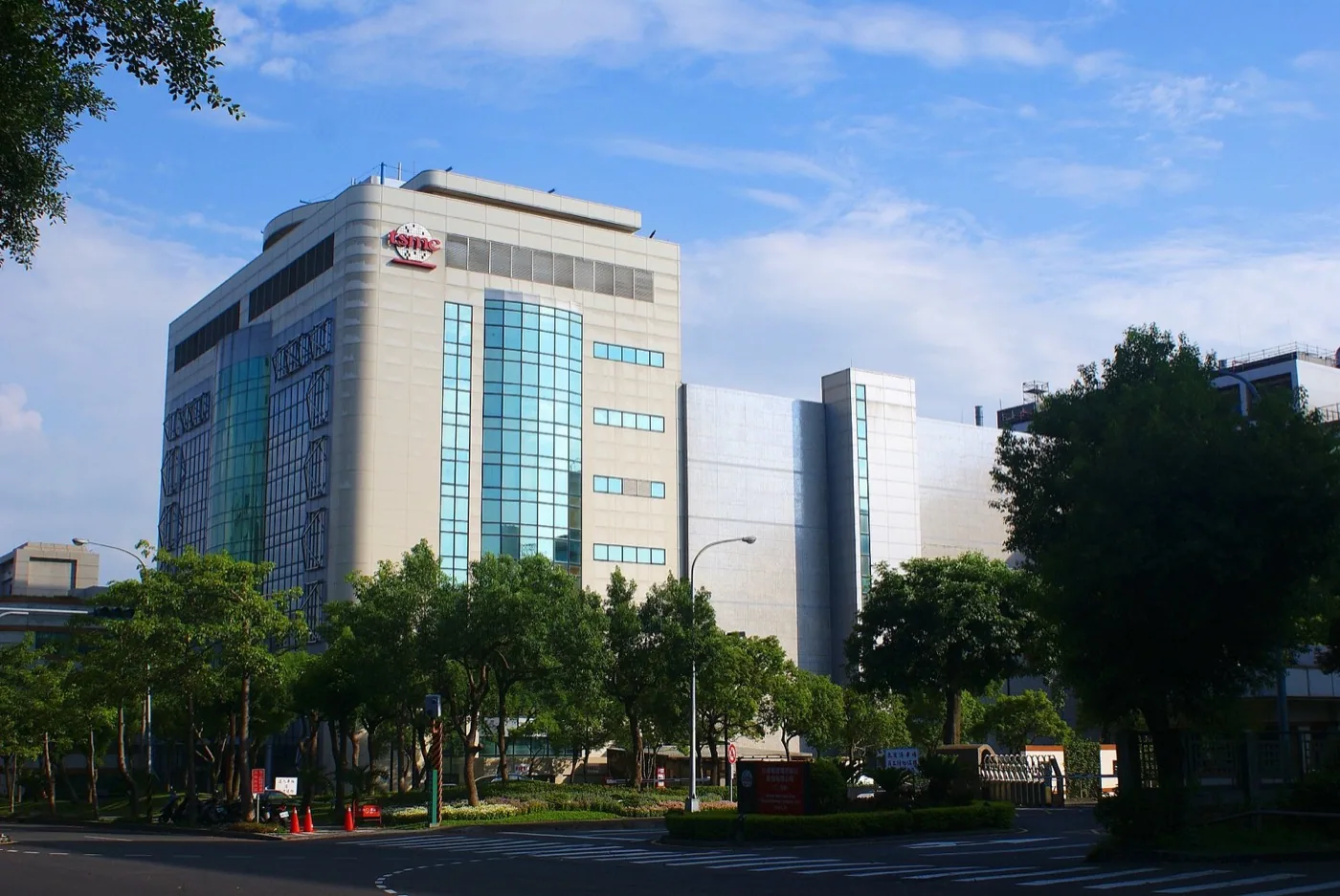
TSMC Fab 5 in Hsinchu Science Park, 2010. Photo: Peellden. License via Wikimedia Commons.
The story begins earlier. In 1973, ITRI spent US$4.5 million to acquire integrated circuit technology from the American company RCA and sent nineteen engineers to the United States for training2. No one at the time imagined that this "tuition" would become the first cornerstone of Taiwan's semiconductor kingdom. In 1980, ITRI transferred technology to establish United Microelectronics Corporation, giving Taiwan its first semiconductor company. But K.T. Li was not satisfied: UMC was too small, its technology lagged international standards, and Taiwan needed a larger breakthrough.
On February 21, 1987, Morris Chang founded Taiwan Semiconductor Manufacturing Company in Hsinchu Science Park and pioneered an unprecedented business model: pure-play foundry.
At the time, the idea sounded absurd. Semiconductor companies worldwide were vertically integrated, handling everything from design to manufacturing. How could a company only manufacture and not design? Would customers really hand over their most confidential blueprints?
Chang's logic was simple: the semiconductor industry was becoming increasingly complex, and design and manufacturing were two entirely different specializations. Rather than doing everything and excelling at nothing, it was better to focus on one thing and make chip manufacturing the best in the world.
TSMC's initial shareholding structure was carefully arranged: the government invested 48.3%, private investors 24.2%, and Philips of the Netherlands held 27.6%4. Philips's participation was crucial. At the time, the semiconductor industry was dominated by the United States and Japan, and Europe urgently needed alternative suppliers. Philips not only invested; it also gave TSMC its own chip orders, becoming its first major customer.
The foundry model triggered a great division of labor in the semiconductor industry: IC design companies concentrated on designing chips, such as Qualcomm, NVIDIA, and MediaTek; foundries concentrated on manufacturing, such as TSMC, UMC, and GlobalFoundries; and assembly and testing companies handled back-end processes, such as ASE and SPIL. In the past, only giants like Intel and IBM could afford the astronomical investment required for fabs. Now any startup with a good idea could design a chip and then have TSMC manufacture it.
The core of the foundry model is trust. Customers must believe that TSMC will not steal their designs, leak trade secrets, or compete with them. TSMC established a set of four "rules of trust": technological neutrality, meaning it would never design chips itself; customer equality, meaning all customers would receive the same technology and service; the strictest confidentiality agreements; and fair capacity allocation. These rules have been enforced for nearly forty years, without exception.
📝 Curator's note: In Taiwan in 1987, the nineteen engineers ITRI had sent out through the RCA program were only just in their early forties. They had learned American silicon processes from the 1960s, and no one at the time could have predicted that thirty years later they would become the party that defined the world's packaging technology requirements. TSMC's decision not to design chips itself, a clause of "voluntary castration," unexpectedly became the lock-in that Jensen Huang, Tim Cook, and Lisa Su could not escape. The greatness of the foundry model lies not in what it did, but in what it chose not to do. Push the origin further back: Bell Labs invented the transistor in 1947; Texas Instruments and Fairchild each produced integrated circuits in 1958; and the Nationalist government's relocation to Taiwan in 1949 brought a group of technically trained bureaucrats who later became the backbone of ITRI. RCA's US$4.5 million was the baton, not the starting line.
Burn J. Lin and ASML: The Bet by Two Children in Water Lithography
Foundry was never only about TSMC. Reader @malathrone_21k_running added a crucial historical line in the comments: sharing the same Philips bloodline as TSMC was ASML, the lithography company spun out of Philips in the Netherlands in 1984. Today, it is the world's only supplier of EUV, or extreme ultraviolet, machines. Thirty years ago, both companies were children overlooked by industry giants5.
The key figure in the story is a Taiwanese engineer named Burn J. Lin. Starting in 1992, he worked on lithography technology at IBM's Watson Research Center; in 2000, he returned to Taiwan and joined TSMC as head of R&D6. At that time, the next lithography route was contested. Nikon and Intel bet on 157-nanometer deep ultraviolet, but 157nm ran into problem after problem: calcium fluoride lenses suffered birefringence, thin films absorbed too strongly at that wavelength, and process integration was difficult7.
At the SPIE optics conference in 2002, Lin proposed a radical idea: "Keep the 193-nanometer light source, but fill the space between the lens and the wafer with water." Water has a refractive index of 1.44, making 193-nanometer light equivalent in water to roughly 134-nanometer resolution, finer than 157nm, without changing the light source or lenses8.
Nikon did not believe it and continued betting on 157nm. ASML was willing to gamble. It, too, was a child looking for a physical lever to reverse its position, just like TSMC. In 2003, ASML began developing 193nm immersion lithography, or 193i, machines. In 2007, it led the world in mass production, carrying lithography from the 65-nanometer node through six generations until EUV took over89.
"Nikon did not dare to do immersion because it feared heat, so ASML and we had to do it ourselves." This technical route pushed Nikon off the throne of lithography machines9. Thirty years ago, two children each placed a bet. Today, one is the world's only EUV machine maker, and the other is the world's only 2-nanometer foundry. The two seeds Philips scattered in the Netherlands met again on the twenty-first-century stage.
A Fifty-Year Materials Genealogy: From Silicon to Gallium Nitride to Topological Superconductors
To understand the semiconductor battlefield of 2025, one must first understand a physical line that has never been clearly explained.
Silicon is the starting point of that line. Its "bandgap" is 1.1 electron volts, or eV, the minimum energy ticket an electron must pay to jump from the valence band to the conduction band. A small bandgap makes chips easier to build, but it has two ceilings: high voltage causes breakdown, and high frequency generates heat. PanSci states this limit plainly: "The operating frequency limit of silicon-based semiconductors is only below 100k. If it exceeds 100k, conversion efficiency drops sharply, and serious energy waste occurs."10
Gallium nitride's bandgap is 3.4 eV, three times that of silicon; its breakdown voltage limit is ten times higher than silicon's; and its operating frequency can be pushed to 1000K, a full order of magnitude above silicon10. Translate these physical numbers into daily life: at the same power, a gallium nitride transformer's inductor coil can be much smaller, and its heat dissipation requirements are much lower. That is how fast chargers small enough to fit in the palm of a hand were born.
Silicon carbide takes another path. It is also a wide-bandgap material, with a bandgap of 3.26 eV, but it better tolerates high temperature and high voltage. PanSci identifies its battlefield directly: "Silicon carbide has good stability under high temperature and high voltage. Especially as demand for fast charging of future electric vehicles increases, charging demand above 1000 volts will make silicon semiconductors, which can only withstand 600 volts, unable to cope; silicon carbide is expected to take over key components in electric vehicles."10
💡 Did you know: A semiconductor's "bandgap" determines how much voltage it can bear, how fast a frequency it can run, and how much heat it generates. Silicon's 1.1 eV has been the foundation of consumer electronics for fifty years; gallium nitride's 3.4 eV supports 240-watt phone fast charging; silicon carbide's 3.26 eV enters 800-volt electric vehicle inverters; the next stop may be 5.5 eV diamond semiconductors. The entire materials genealogy is a staircase of rising energy density. Each step Taiwan climbs requires another negotiation with the physical limits of materials science.
The next stop has not yet been named: it may be diamond, carbon with a 5.5 eV bandgap; gallium oxide, Ga₂O₃, at 4.8 eV; or a move into an entirely different physical mechanism, such as the topological superconductor, the path Microsoft announced in February 2025 with its Majorana 1 quantum processor11. When the physics changes, the entire industry chain is rewritten with it.
The Gallium Nitride in Your Fast Charger
Pull the camera back to your backpack.
The Nokia 3310 charger was 4.56 watts. A fast charger in 2025 can reach 240 watts. That is a 52-fold difference. PanSci has mapped this timeline: "Today's hottest gallium nitride fast chargers reach 65 watts, a 13-fold difference; ideally, charging time would also be shortened to one-thirteenth."10 Even more striking, the Chinese brand realme launched the 240-watt ultra-fast-charging GT Neo5 in early 2023, pushing the multiple above fifty.
Physically, this growth curve depends on switching to gallium nitride, while copper wire thickness and battery volume are shrinking instead. The most direct way to increase power while reducing volume is to raise the operating frequency. But "the operating frequency limit of silicon-based semiconductors is only below 100k"10. This is PanSci's "limit of silicon." Gallium nitride pushes the operating frequency above 1 MHz, allowing transformers and inductors to shrink in tandem, so the entire charger can fit into a pocket.
The problem is that just as Taiwan's fast-charging market was about to explode, TSMC announced something: it would exit GaN foundry services in July 202712.
Two pressures lie behind this decision. First, Chinese GaN manufacturers, including CR Micro, Silan Microelectronics, and Innoscience, expanded capacity aggressively, pushing foundry prices to levels TSMC did not want to accept. Second, AI chips were simply too profitable, and TSMC wanted to convert GaN fab space into advanced packaging, or CoWoS, production lines. Technology licenses went to Vanguard International Semiconductor, or VIS, and GlobalFoundries. The burden of Taiwan's GaN foundry work was handed to companies such as WIN Semiconductors, 3163, and Advanced Wireless Semiconductor, 8086, which had begun betting on this field a decade earlier12.
⚠️ Contested view: There are two interpretations of TSMC's exit from GaN foundry services. One camp sees it as a rational choice to "reserve capacity for AI": the profit on a single 3-nanometer wafer is more than twenty times higher than that of a 6-inch GaN wafer, so capacity allocation naturally goes toward higher returns. The other camp questions whether Taiwan is surrendering the next-generation foundation of consumer electronics, including phones, laptops, and chargers, to Chinese manufacturers by giving up GaN. Is the "shield" in the silicon shield now only the AI segment? The difference between the two camps is this: do you believe the value of the sacred mountain protecting the nation lies in "irreplaceable leading-edge process technology," or in "a complete cluster across the entire supply chain"?
Whether TSMC, the wafer giant GlobalWafers, or major semiconductor companies at home and abroad, all have long since boarded this train10. But which carriage to ride is a separate question.
GlobalWafers' 8-Inch SiC Wafers
If gallium nitride is the story of phone fast charging, silicon carbide is the story of electric vehicles.
The core company in Taiwan's SiC line is GlobalWafers, not TSMC. In 2024, GlobalWafers raised monthly capacity for 6-inch SiC wafers to about 20,000 pieces, expanded its self-developed crystal growth furnaces from three to twenty, and pushed yield above 50%13. In 2025, it began mass production of 8-inch SiC wafers, the first company in Taiwan to do so.
GlobalWafers CEO Doris Hsu has always spoken directly: "Sino-American Silicon Products is forming a 'virtual IDM group' to target silicon carbide demand over the next five years. We are catching up fast."13 The strategy is to bind parent company Sino-American Silicon's crystal growth, through GlobalWafers; epitaxy, through Actron; and modules, through Hestia Power, into one chain.
But SiC is not a straight upward story. In the second half of 2025, Chinese SiC manufacturers, including Sanan Optoelectronics and Tankeblue, expanded wildly, creating global oversupply. GlobalWafers' 6-inch and 8-inch SiC capacity utilization once fell below 50%14. Compared with PanSci's optimistic 2023 prediction that "electric vehicle demand will take over," this script added a trough.
The signal of recovery comes from NVIDIA. Rumor has it that NVIDIA's next-generation Rubin GPU platform will use SiC in the interposer, paired with an 800-volt high-voltage direct current data center architecture, with full mass production in 202714. If this rumor proves true, GlobalWafers' 8-inch SiC capacity will be redirected from electric vehicles to AI data centers, and the entire story will light up again.
📝 Curator's note: Gallium nitride and silicon carbide are often grouped as "third-generation semiconductors," but in Taiwan this category has industrial significance beyond the label of "next-generation materials." It represents the first semiconductor domain in which Taiwan can have a complete supply chain around, not through, TSMC. GlobalWafers grows crystals, Episil manufactures, WIN Semiconductors packages, and Advanced Wireless Semiconductor designs. Beyond the sacred mountain protecting the nation, a much quieter but independent "third-generation mountain range" is growing.
The Jensen Huang and CoWoS+ Lock-In
Back to the AI battlefield.
NVIDIA's H100 GPU uses TSMC's 4-nanometer process and CoWoS-S packaging to integrate HBM3 high-bandwidth memory. Blackwell B200 upgrades to CoWoS-L, integrating two Blackwell GPUs and one Grace CPU, with AI training speed four times faster than H10015. The next generation, Rubin, is expected to launch in 2026.
The core of every GPU generation is the twin engine of "advanced process + advanced packaging." Process technology makes transistors smaller and smaller; packaging stacks different dies closer and closer together. PanSci explained this through a comparison between Taiwan's winding Provincial Highway 9 and the Hsuehshan Tunnel: "Traditional packaging requires traveling along the winding Provincial Highway 9, while advanced packaging cuts straight through, opening the Hsuehshan Tunnel that connects the two places, making data movement more convenient and faster."16
The core of CoWoS, Chip-on-Wafer-on-Substrate, is the through-silicon via, or TSV: different dies are stacked together, and vertical microscopic channels run through the silicon substrate, turning two originally separate circuits into a three-dimensionally connected system. PanSci describes it plainly: "Three-dimensional stacking can place chip C above chip A and, through through-silicon via technology, penetrate the thinned silicon substrate with ultra-high-density vertical interconnects to connect the two circuits; the distance between them changes from worlds apart to close at hand."16
The capacity numbers are even sharper. TSMC's monthly CoWoS capacity was about 35,000 wafers at the end of 2024, with a target of 75,000 by the end of 2025 and 150,000 by 2028, implying a compound annual growth rate of nearly 80%17. NVIDIA has directly booked TSMC's CoWoS capacity through 2027, and all chips, regardless of which TSMC fab produces them, including Arizona, must ultimately be sent back to Taiwan for CoWoS packaging17.
This is the dual monopoly of Jensen Huang and TSMC. NVIDIA controls design, while TSMC controls manufacturing and packaging. Together, the two companies hold the key node of AI data centers.
On June 2, 2024, at his Computex keynote in National Taiwan University's Sports Center, Jensen Huang publicly laid out this lock-in for the world. The slides showed the Blackwell and Rubin roadmaps, but behind every slide stood TSMC's CoWoS production lines.
NVIDIA official channel: Jensen Huang's June 2, 2024 Computex keynote, "The Era of AI," at the NTU Sports Center. Across two hours, he laid out Blackwell GPUs, NVLink, and Spectrum-X one slide after another, but the physical site behind every slide was Baoshan, Hsinchu. He did not say, "Without TSMC, there is no NVIDIA," but every capacity chart said it for him.
The physical costs of 3D packaging are substantial. PanSci has pointed out the difficulties: "Advanced packaging has very high requirements for die flatness and chip alignment. If during stacking some contacts fail to connect and conduct properly, yield loss occurs. Moreover, integrated circuits produce energy loss during computation, raising temperature; advanced packaging brings dies closer together, so heat conduction affects them mutually. Everyone warms one another, making heat dissipation even more difficult."16
The next stages are SoIC, System on Integrated Chips, and SoW-X, System on Wafer. SoIC is "true 3D": direct wafer-on-wafer stacking without bumps. SoW-X is expected to enter mass production in 2027. Its reticle size is 9.5 times that of current CoWoS, integrating more than sixteen large computing chips and delivering computing power forty times higher than existing CoWoS17. As AI chips grow larger, TSMC's packaging lines increasingly resemble small factories.
ALD: Growing Atom by Atom
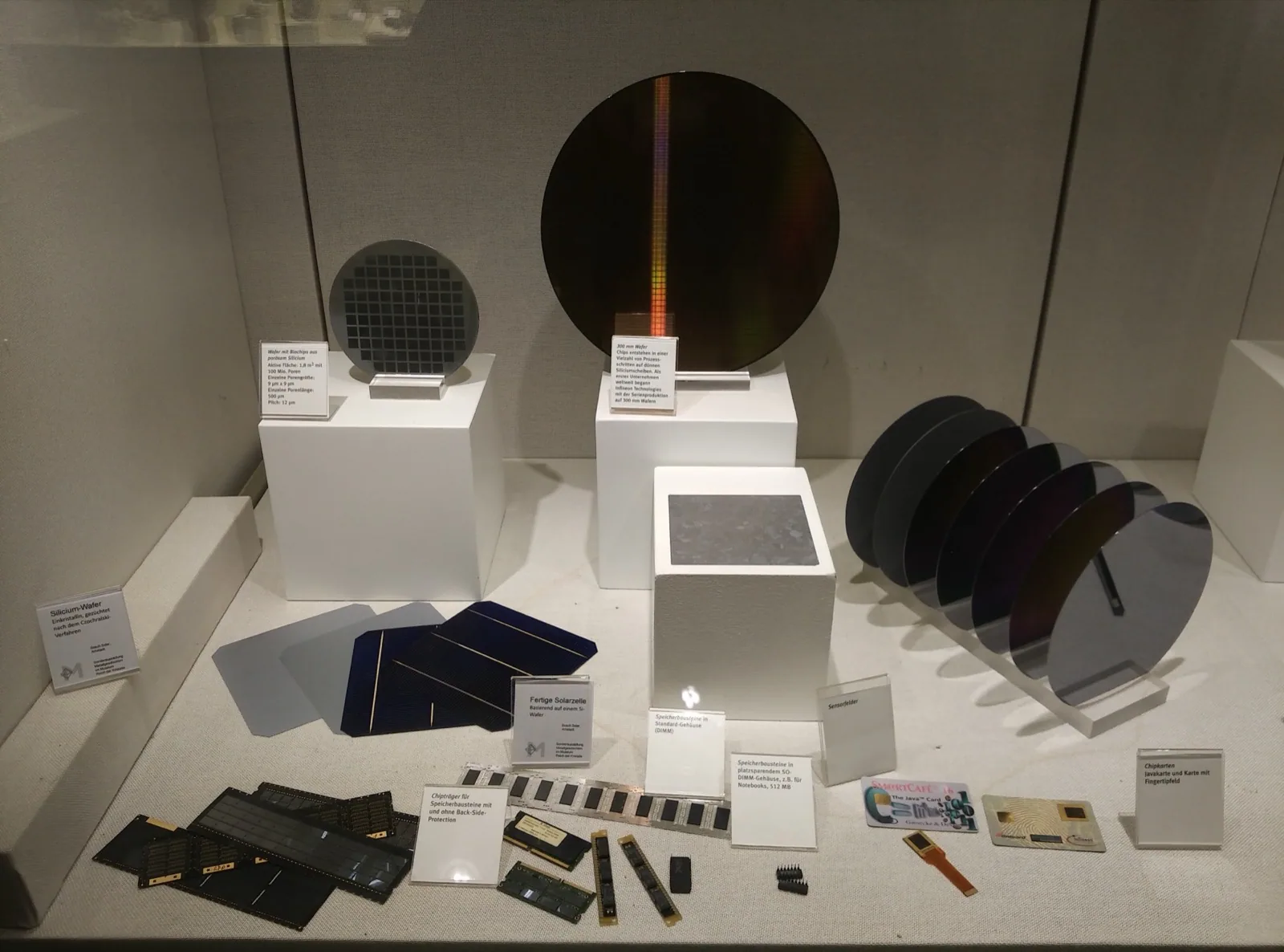
Silicon wafer sample display, 2017. Photo: ArticCynda. License via Wikimedia Commons.
3 nanometers, 2 nanometers, 1.6 nanometers. Behind these numbers is a quiet but crucial manufacturing technology: atomic layer deposition, or ALD.
ALD was invented by a Finn, but it became an unavoidable core step for every advanced-process wafer in Taiwan.
The story begins in Finland. In 1974, materials scientist Tuomo Suntola began developing ALD at the Finnish company Instrumentarium Oy; by 1977, the technology had taken shape and made its first public appearance in an industrial demonstration18. At the time, the technology was only meant to make electroluminescent displays. Suntola himself did not expect that thirty years later it would become the lifeline of nanoscale processes. In 1999, he sold ALD technology to the Dutch semiconductor equipment company ASM; today, ASM holds more than 55% of the ALD market18.
PanSci explains ALD's principle cleanly: "Atomic layer deposition is an improved chemical vapor deposition technology. It divides the deposition process into two steps. First, the first precursor is injected and reacts with the substrate surface... After the surface is saturated, the second precursor is injected and reacts with the precursor already attached to the surface, forming the target material and completing the thin-film process."18 The two precursors are injected one after the other, and each cycle grows only one atom-thick layer of film.
Why does this matter? Because the gate thickness of a 2-nanometer transistor is down to only a few atoms, and the gate insulating layer must achieve atomic-level flatness and atomic-level thickness control. Traditional chemical vapor deposition, or CVD, cannot do this. Physical vapor deposition, or PVD, cannot do this. Only ALD can "grow it layer by layer." Every one of TSMC's advanced-process fabs contains ASM ALD machines. This chain of Dutch equipment, Finnish technology, and Taiwanese process engineering is the physical foundation that makes 2-nanometer mass production possible.
💡 Did you know: The smallest feature size in a 2-nanometer process is roughly the width of twenty silicon atoms placed side by side. If silicon atoms were enlarged to the size of table tennis balls, a 2-nanometer transistor would be about the length of a table tennis table. ALD's job is to cover that table with insulating material, "one ball at a time."
ASM is not listed in Taiwan, but nearly all of the largest customers for its 12-inch ALD machines are in Taiwan. This supply chain is invisible but irreplaceable. If TSMC's 2-nanometer mass production falters, there is no second ALD company in the world that can fill the gap.
After 2nm Comes Quantum
The story after the angstrom scale, where 1 nanometer equals 10 angstroms, has not yet been fully written by TSMC.
In the fourth quarter of 2025, TSMC began 2-nanometer mass production at Kaohsiung Fab 22, with Hsinchu Baoshan Fab 20 following afterward1. The 2-nanometer node adopts GAA, or Gate-All-Around, nanosheet transistor architecture for the first time, abandoning the FinFET architecture used from 22 nanometers all the way to 3 nanometers19. Two nanometers is equivalent to the width of twenty silicon atoms and is already approaching theoretical physical boundaries. The first customers include Apple's A-series chips and NVIDIA's AI chips, and 2-nanometer capacity will expand quarter by quarter20.
The next stop is 1.6 nanometers, or A16, expected to enter mass production in the fourth quarter of 2026. It introduces backside power delivery network technology for the first time, which TSMC calls Super Power Rail19. At the same power, it is 10% faster than N2P; at the same performance, it saves 15-20% power.
But what comes after 1.6 nanometers? The lower process nodes go, the more expensive they become. R&D cost for 28 nanometers was about US$1 billion; 7 nanometers jumped to US$3 billion; 3 nanometers soared to US$10 billion; and 2 nanometers is estimated to exceed US$20 billion21. The exponential curve of Moore's Law turns late-stage R&D costs astronomical, which is also why PanSci says "the complexity and capital investment of advanced process development increase exponentially, and investment and return often fail to remain proportional."16
So the semiconductor industry changed strategy: horizontal expansion became vertical stacking, or 3D packaging; silicon became new materials, such as GaN and SiC; and eventually computing may switch to an entirely different physics, such as quantum computing.
Academia Sinica's timeline unfolded this way. In October 2023, a 5-qubit superconducting quantum computer was completed; on January 29, 2024, President Tsai Ing-wen visited, and the quantum computer officially went online3. PanSci wrote: "In January 2024, Taiwan's first independently developed quantum computer was officially born at Academia Sinica. Although it had only five qubits, it opened the prelude to Taiwan occupying a place in the global quantum computer arena."22
In December 2025, a 20-qubit superconducting quantum chip was completed; in January 2026, online access was announced3. Coherence time, T1, jumped from 15-30 microseconds in the 5-qubit era to 530 microseconds for the 20-qubit chip. Coherence time is the duration for which a qubit can maintain a superposition state. The longer it is, the less noise there is and the more complex the computation can be.
The cross-ministerial national quantum team was formally established in March 2022, with a five-year budget of NT$8 billion and seventeen research teams23. In April 2026, the Ministry of Economic Affairs established the Quantum Industry Technology Promotion Office to bridge academic R&D and industry.
What ITRI is doing is especially interesting: using TSMC's 28-nanometer process to make "control chips for qubits." Central News Agency quoted ITRI in March 2024: "Using Taiwan's strengths in microwave IC design and TSMC's 28-nanometer process, [ITRI] has built low-temperature, 4K or -269°C, control chips and modules... shrinking control instruments, placing them inside low-temperature refrigerators, reducing overall equipment volume by 40%, simplifying wiring, and providing commercialization advantages... The module's power consumption is more than 50% lower than data published by major international companies."24
📝 Curator's note: Taiwan's quantum strategy is not to build qubits itself, which is the territory of IBM, Google, and Academia Sinica. It is to miniaturize control circuits until they can be placed inside dilution refrigerators. From 5 qubits to 20 qubits, ITRI's control chips have moved from supporting 1 qubit, to 2 qubits, to 8 qubits, with a target of 20 qubits in 2026-2027. The next stop for the sacred mountain protecting the nation is to become the foundry of the quantum era, not to personally compete for quantum supremacy. But no one has yet hammered down the stake that says, "Leave it to Taiwan."
Three Quantum Routes: Superconducting, Ion Trap, and Topological
There is not only one path to quantum computers.
Superconducting qubits are the route pursued by IBM, Google, and Academia Sinica. Their advantage is process compatibility with existing semiconductor fabs, which is where Taiwan has a possible role, and fast control speed. Their disadvantage is the need for dilution refrigerators close to absolute zero, 15 mK, about -273°C, and high noise. In 2019, Google used its 53-qubit Sycamore processor to declare quantum supremacy, completing in 200 seconds a task that would take a traditional supercomputer 10,000 years25.
Trapped ion qubits follow the path of using lasers to control individual atoms. PanSci has summarized the difference in this route: "Ion trap technology uses lasers to control individual atoms for computation. This technology has extremely high precision and stability, but it also faces problems of technical complexity and cost."22 Representative companies include IonQ and Quantinuum. The advantages are high precision, good stability, and no need for extremely low temperatures. The disadvantages are slow control speed and difficulty scaling to large numbers of qubits.
Topological qubits are Microsoft's next-generation bet. In February 2025, Microsoft announced the Majorana 1 topological quantum processor, claiming it could scale to one million qubits11. In theory, topological qubits have extremely strong resistance to interference, but this route is the least mature. The existence of Majorana particles themselves is still being verified in physics.
Each of these three routes carries risks. Taiwan's strategy is to ensure that no matter which route wins, Taiwan has a supply-chain node, rather than betting that any single route will prevail. The superconducting route depends on TSMC 28-nanometer control chips; the precision optics needed by the ion trap route overlaps with Taiwan's optoelectronics industry; and if the topological route succeeds, it will still require films of extreme purity, leading back again into ALD territory.
Are Overseas Fabs Expansion or Export?
TSMC's globalization accelerated in the 2020s.
Arizona Fab 21 in the United States: Phase 1, 4-nanometer process, enters mass production in the first half of 2025; Phase 2, 3-nanometer and 2-nanometer processes, enters mass production in the second half of 2027; Phase 3, 2-nanometer and A16, is expected before 2030. Total capital expenditure is about US$165 billion26. But there is an important "but": CoWoS packaging for all AI chips remains in Taiwan. Wafers produced in Arizona will be sent back to Taiwan for packaging17.
Kumamoto Fab 1 in Japan: 22-28 nanometer processes, mass production in 2024, in cooperation with Sony and Toyota. The schedule for the originally planned Fab 2, at 12-16 nanometers, is uncertain, with some resources reallocated to Arizona.
ESMC in Dresden, Germany, where TSMC holds 40%: automotive chips at 28, 22, 16, and 12 nanometers; equipment move-in in the second half of 2025; mass production in 2027; monthly capacity of about 40,000 wafers27.
These overseas fabs share an "N-2 principle": they always lag Taiwan's domestic fabs by two generations. When Taiwan is producing 2 nanometers domestically, the most advanced overseas node is 4 nanometers; when Taiwan pushes 1.6 nanometers, overseas fabs have only reached 3 nanometers. This red line is written into the engineering ethics of geopolitics, not into contract clauses.
⚠️ Contested view: Are overseas fabs an expansion or dilution of the silicon shield? Supporters say that keeping technology in Taiwan while expanding capacity overseas turns the silicon shield from "one island" into "one chain," making derisking more complete. Opponents say that every overseas fab exports a cohort of trained engineers, a set of mass-production SOPs, and a share of customer relationships. Thirty years from now, when Arizona or Kumamoto accumulates experience up to the N-2 boundary, the line of "the most advanced two generations" may slowly be compressed. The N-2 principle is currently TSMC's commitment, not a law of physics.
Proceeding alongside overseas fabs is the "outflow of design talent." AI chip design needs not only Taiwan; Silicon Valley, Tel Aviv, and New Delhi all have their own design centers. TSMC's foundry ecosystem is moving from "island-wide engineers" to a hybrid of "global engineers + island-wide manufacturing."
Environmental Costs: The Other Side of the Sacred Mountain
The sacred mountain protecting the nation has weight.
Water is the most intuitive issue. TSMC's three major science parks consume more than 208,000 metric tons of water per day. Environmental groups estimate that after new fabs enter production in 2025, water use could increase fourfold to 770,000 metric tons per day28. TSMC's response is that every drop of water is used an average of 3.5 times, the recycling rate reaches 87%, new fabs target 90%, and 5.54 million cubic meters of additional water savings were achieved in 2024.
Electricity is the second issue. A single 3-nanometer fab consumes about 2.1 billion kWh of electricity annually, equivalent to the yearly electricity consumption of 20,000 households in Taiwan. Power consumption at 2 nanometers and 1.6 nanometers will continue to rise. TSMC has pledged to reach RE100, or 100% renewable energy, by 2050, but Taiwan's green electricity supply cannot keep pace with semiconductor expansion. This timeline is constantly being stress-tested.
Working hours are the third issue. The hours, housing prices, and birth rates of engineers in Hsinchu Science Park belong in another article. But like materials science, they are also a physics problem: human time and energy have a "bandgap" too. Once the threshold is exceeded, breakdown occurs.
The existence of the sacred mountain protecting the nation depends not only on TSMC's technology, government policy, and geopolitical opportunity, but also on the costs borne collectively by 170,000 science park engineers, an entire supply chain of companies, and every Taiwanese resident who uses electricity and water.
A Complete Ecosystem: Taiwan Is Not Only TSMC
The competitiveness of Taiwan's semiconductor industry comes from the entire cluster, not from TSMC alone. On the IC design side are MediaTek, one of the global top three, Novatek, Realtek, and Himax. In wafer foundry, beyond TSMC, there are UMC, Vanguard International Semiconductor, and Powerchip Semiconductor Manufacturing. Back-end assembly and testing are handled by ASE, the world's largest, SPIL, and King Yuan Electronics. Third-generation semiconductors are supported by GlobalWafers for SiC crystal growth, Episil, WIN Semiconductors for GaN, and Advanced Wireless Semiconductor. Memory is carried by Nanya Technology and Winbond. On the equipment and materials side, invisible companies such as Gudeng Precision, Scientech, and Topco fill key gaps.
A chip can go from design to completion by circling Taiwan once, without cross-border transport. This "short-chain advantage" was seen by the whole world during COVID and has since been written into the supply-chain white papers of every technology giant.
Hsinchu Science Park was established in 1980. Over more than forty years, it has accumulated more than 500 companies and 170,000 workers. An engineer might spend five years at TSMC, jump to MediaTek to design chips, and then move to ASE to handle packaging. This cross-company circulation of talent effectively diffuses technical standards across the entire industry.
What about competitors? Samsung of South Korea invested US$230 billion from 2022 to 2026 in a vertical integration strategy, but its advanced-process yields still lag TSMC21. Intel was stuck for years at 10 nanometers; in 2021, it proposed IDM 2.0, hoping to combine design and foundry services, but by 2025 its foundry business had not secured major customers. Most ironic of all, some of Intel's own high-end chips shifted to TSMC for foundry manufacturing.
The Quantum Position Remains Open
The Nokia 3310 charger was 4.56 watts. A fast charger in 2025 is 240 watts. That is a 52-fold difference. Silicon took thirty years to travel that road; gallium nitride completed the rest in five.
Inside Academia Sinica's quantum laboratory, superconducting quantum chips must operate at 15 millikelvin, about -273°C. ITRI's control chips, made using TSMC's 28-nanometer process, compress the "control instrument volume" required for this ultra-low temperature from a building into a small box. Taiwan's semiconductor capabilities are moving the boundary of quantum computers, bit by bit.
But no one can say clearly where that boundary lies. Qubit coherence time has gone from 15 microseconds to 530 microseconds, and this is only the beginning. The nineteen engineers sent out under the RCA program fifty years ago probably did not know either that their 1973 would crystallize into 2 nanometers in 2025.
The sacred mountain protecting the nation has dominated the present through fifty years of foundry experience. For the next fifty years, Taiwan has not yet secured its foundry position in the quantum era.
✦ Jensen Huang's Blackwell performs inference in the cloud above your head; GlobalWafers' SiC wafers heat up inside the electric vehicle charging post by your door; the first ALD film Tuomo Suntola made in Finland in 1974 seals the gate insulating layer inside your phone's chip. Semiconductors have always been fifty years of an entire materials genealogy climbing step by step along bandgap physics, not the property of TSMC alone. Physics will tell us where the next step is. Whether to climb it is Taiwan's choice.
Where this story traveled
Further Reading:
- Taiwanese Company: TSMC — The corporate governance, financial structure, and capital expenditure scale of the sacred mountain protecting the nation
- Taiwanese Company: MediaTek — How the IC design leader positions itself in phone chips and AI edge computing
- Taiwanese Company: ASE Semiconductor — The world's largest assembly and testing industry player, and the back-end process ecosystem beyond CoWoS
- Mountain Makers: A Gamble of the Century — Hsiao Chu-chen's 2025 documentary, based on five years of interviews with 80-plus semiconductor predecessors; in 2026 it entered Purdue, Wisconsin, and Michigan, three CHIPS Act investment strongholds
- Ta-You Wu — While Taiwan was pushing semiconductors in the 1980s, he served as president of Academia Sinica and insisted on the importance of basic science, laying the foundation for Taiwan's research system
- Taiwan's Robotics Industry — Why is the island that leads the world in semiconductors catching up in the robotics era? Reading the industrial gap from the opening of NCAIR
- Taiwan's Stock Market and Capital Markets — How the entire supply-chain ecosystem supporting Taiwan's status as the world's sixth-largest stock market in 2026 appears in capital markets
- Taiwan Artificial Intelligence School — How the ten thousand AI engineers trained by AIA over eight years return to the existing semiconductor and ICT chain and strengthen Taiwan's software side
- Computex: Two of the Three International Computer Shows Are Gone, and the One That Remains Grew in Taipei — TSMC's CoWoS and advanced process nodes shake hands with the world's AI giants every late May at this 45-year-old Taipei computer show
- Taiwan Science Parks — Hsinchu, Tainan, and Taichung Science Parks: the physical substrate of semiconductor clusters and the geographic center of the silicon shield
Image Sources
This article uses three CC / PD licensed images, cached in public/article-images/technology/ to avoid hotlinking source servers:
- Silicon vs GaN 30W USB-C chargers — Photo: 4300streetcar, 2025-12-25, CC BY 4.0, Wikimedia Commons file Silicon_vs_GaN_30W_USB-C_chargers.jpg
- TSMC Fab 5 Hsinchu — Photo: Peellden, 2010-09-05, CC BY-SA 3.0, Wikimedia Commons file TSMC_Fab5.JPG
- Silicon wafers museum display — Photo: ArticCynda, 2017-10-23, CC0 public domain, Wikimedia Commons file Silicon_wafers.jpg
References
- Focus Taiwan 2025/12/30 — TSMC 2nm production — TSMC's 2-nanometer mass production begins primarily at Kaohsiung Fab 22, followed by Hsinchu Baoshan Fab 20↩
- CommonWealth Magazine — K.T. Li and the birth of TSMC — Morris Chang founded TSMC in 1987 and established the "pure-play foundry" model, laying the foundation for global division of labor in semiconductors; background on the 1973 RCA technology transfer for US$4.5 million↩
- Academia Sinica — Announcement on the 20-qubit superconducting quantum chip — Academia Sinica completed a 20-qubit superconducting quantum chip in December 2025 and connected it online on January 29, 2026; coherence time T1 reached 530 microseconds↩
- Semiwiki — How Philips Saved TSMC — Semiwiki research indicates Philips's shareholding was 27.6%; Philips was a crucial shareholder for TSMC's early technology and customers↩
- Wikipedia — ASML Holding — ASML was established on April 1, 1984, as ASM Lithography, a 50/50 joint venture between Philips of the Netherlands and ASM International, ASMI; after its 1995 stock listing, ASMI exited; today ASML is the world's only supplier of EUV lithography machines↩
- Wikipedia — Burn-Jeng Lin — Burn-Jeng Lin was born in Vietnam in 1942, worked on lithography technology at IBM Watson Research Center from the 1970s, and returned to Taiwan in 2000 to join TSMC as R&D head; he received the SPIE Frits Zernike Award in 2008 and is known as the "father of immersion lithography"↩
- Electronics Weekly — Immersion litho sidelines 157nm — The 157nm route was replaced after 2002-2003 by 193nm immersion because of calcium fluoride, CaF₂, lens birefringence, strong thin-film absorption at 157nm, and process integration difficulties; Intel + Nikon's bet failed↩
- Wikipedia — Immersion lithography — Burn-Jeng Lin proposed 193nm immersion lithography at SPIE in 2002; water's refractive index of 1.44 gives 193nm an effective resolution of about 134nm; ASML entered mass production in 2007, carrying lithography from 65nm to 7nm and extending Moore's Law by six generations↩
- CommonWealth Magazine — Interview with the Father of Immersion Lithography Who Put TSMC on the Map — 2024-06-18 interview with Burn-Jeng Lin; historical background on "Nikon did not dare to do immersion"; Lin returned to TSMC in 2000 and promoted adoption of immersion lithography, part of thirty years of technical collaboration between TSMC and ASML↩
- PanSci — Gallium Nitride: Get the Same Power in One-Third the Time — Author: PanSci editorial team. Gallium nitride has a 3.4 eV bandgap, 10x breakdown voltage, and 1 MHz operating frequency versus silicon's 100 kHz; silicon carbide applications in 1000-volt electric vehicle fast charging. Content Curation Partner per MOU 2026-05-05↩
- TechNews — Microsoft announces Majorana 1 topological quantum processor — Microsoft announced the world's first topological quantum processor, Majorana 1, in February 2025, claiming it can scale to one million qubits↩
- TrendForce — TSMC exits GaN foundry by July 2027 — TSMC exits GaN foundry services in July 2027, licensing technology to Vanguard International Semiconductor, VIS, and GlobalFoundries; WIN Semiconductors, 3163, ships about 500 6-inch GaN wafers per month↩
- Fugle Direct — GlobalWafers SiC 8-inch wafers enter mass production in 2025 — GlobalWafers' monthly 6-inch SiC capacity reached 20,000 wafers by the end of 2024; self-developed crystal growth furnaces expanded from 3 to 20, yield > 50%; Doris Hsu's "virtual IDM group" strategy↩
- TechNews — SiC supply chain under pressure — Chinese SiC capacity expansion in 2025 caused GlobalWafers' 6-inch and 8-inch capacity utilization to fall below 50%; NVIDIA Rubin GPU rumored to adopt SiC interposers + 800V high-voltage DC data centers with 2027 mass production↩
- SemiAnalysis — NVIDIA Blackwell CoWoS-L Analysis — NVIDIA Blackwell B200 uses CoWoS-L to integrate 2 Blackwell GPUs + 1 Grace CPU; AI training speed is 4x faster than H100; NVIDIA books TSMC CoWoS capacity through 2027↩
- PanSci — Three-Dimensional Stacking: How Advanced Packaging Lets Chips Enter the Hsuehshan Tunnel — Author: PanSci editorial team. Principles of CoWoS / SoIC / TSV through-silicon vias; Provincial Highway 9 vs Hsuehshan Tunnel metaphor; 3D packaging yield and heat dissipation challenges. Content Curation Partner per MOU 2026-05-05↩
- Digitimes — TSMC CoWoS capacity expansion plan — TSMC CoWoS monthly capacity: 35,000 wafers at end-2024, 75,000 by end-2025, 150,000 target by 2028; NVIDIA books capacity through 2027; Arizona wafers sent back to Taiwan for packaging↩
- PanSci — ALD Atomic Layer Deposition: A Fifty-Year Thin-Film Revolution — Author: PanSci editorial team. ALD was developed by Suntola at Instrumentarium Oy in 1974, matured in 1977, and sold to ASM in 1999; ASM holds 55% market share; dual-precursor principle in chemical vapor deposition. Content Curation Partner per MOU 2026-05-05↩
- TSMC official website — A16 (1.6nm) process announcement — 2nm adopts GAA nanosheet transistors for the first time, abandoning FinFET; A16 introduces backside power delivery network, Super Power Rail, for the first time, with Q4 2026 mass production, 10% faster than N2P at the same power and 15-20% lower power at the same performance↩
- Business Next — TSMC 2nm officially enters mass production — TSMC begins 2-nanometer mass production in Q4 2025; specific monthly capacity figures are external industry estimates and have not been officially disclosed↩
- TechNews — TSMC 3nm utilization reaches 100% — Industry estimates suggest TSMC's advanced-process yields outperform competitors; specific yield figures are third-party estimates, not official disclosures↩
- PanSci — Taiwan Quantum Technology: From 5 Qubits to the Mass-Production Era — Author: PanSci editorial team. Academia Sinica's 5-qubit quantum computer was born in January 2024; three routes of superconducting vs ion trap vs topological; Google's 53-qubit Sycamore solved a 10,000-year problem in 200 seconds. Content Curation Partner per MOU 2026-05-05↩
- iThome — National quantum team receives five-year NT$8 billion budget — Cross-ministerial national quantum team established in March 2022, with a five-year NT$8 billion budget and seventeen research teams; Ministry of Economic Affairs established the Quantum Industry Technology Promotion Office in April 2026↩
- Central News Agency 2024/03/06 — ITRI quantum control chip — ITRI uses TSMC's 28-nanometer process to build 4K, -269°C, low-temperature quantum control chips, reducing volume by 40% and power consumption by more than 50% compared with major international companies; development path from 1 qubit in 2024 to 20 qubits in 2026-2027↩
- TechNews — Google Sycamore quantum supremacy — In 2019, Google's 53-qubit Sycamore quantum computer achieved quantum supremacy, completing in 200 seconds a computational task that would take a traditional supercomputer 10,000 years↩
- SemiAnalysis — TSMC Arizona Fab 21 investment plan — TSMC Arizona Fab 21 three-phase investment of US$165 billion; Phase 1, 4nm, enters mass production in 2025; Phase 2, 3nm/2nm, in 2027; Phase 3, 2nm/A16, before 2030; N-2 principle means overseas fabs always lag Taiwan by two generations↩
- Digitimes — ESMC Dresden mass production in 2027 — TSMC holds 40% of ESMC; Dresden, Germany automotive chip fab at 28/22/16/12 nanometers, equipment move-in in H2 2025, mass production in 2027, monthly capacity about 40,000 wafers↩
- CommonWealth Magazine — TSMC water consumption — TSMC's three major science parks consume more than 208,000 metric tons of water per day; environmental groups estimate that after 2025, new fabs could raise water use to 770,000 metric tons per day; TSMC responds that each drop of water is used 3.5 times, recycling rate is 87%, new fabs 90%, and 5.54 million cubic meters of additional water savings were achieved in 2024↩